Common Data : VDD = 1.8V , Lmin = 0.18µm, µ0N = 350cm2/V s, µ0P = 100cm2/V s,
|VTH | = 0.55, tox = 3.8nm, λ = 0.07V−1, χ = 0.1.
1.Consider circuits shown in Fig. 33. Which of these source degenerated circuits have higher input referred noise voltage, and by what factor?
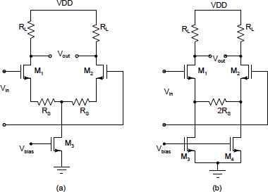
Figure 33 : Source Degenerated Circuits
2. Design circuit in Fig. 34 for an input referred thermal noise voltage of
 and maximum output swing. Assume
 and
and 

Figure 34: Common Gate Stage
4. Assume  Fig. 36. If the contribution of
  to the input referred noise voltage must be one-fifth of that of
  , what is the maximum output voltage swing of the amplifier?
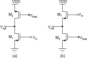
Figure 36 : (a) Common Source Amplifier (b) Source Follower
This problem is to be attempted similar to the problem 5 of the tutorial, i.e., by closing the cap and subtracting the contribution due to the cap. The divergence being 3, the flux from the closed cone is 3 times the volume of the cone which gives  The contribution from the top face (which is a disk of radius 2 ) is
  . Thus the net flux is zero. (You can also try to get this result directly as done in problem 4, where we showed that the flux from the curved surface is zero).
5. Consider the circuit of Fig. 37 - Fig. 38. To decrease overall noise of circuit,
- Whether transconductance of should be kept high or low in two cases of Fig. 37?
Figure 37 : (a) Common Source Amplifier (b) Inverter
- Whether
 should be minimized to reduce noise in Fig. 38?
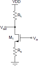
Figure 38 : Source Degenerated Stage
6. Consider input stage of op-amp shown in Fig. 39,
- Should transconductance of be decreased to decrease input-referred thermal noise?
- How sizing of and
 should be done to reduce flicker noise?
Figure 37 : (a) Common Source Amplifier (b) Inverter
Solution :
Part (a)
Step 1: Find gains from each noise source to the output node.
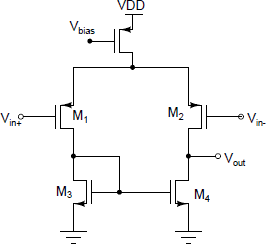
Figure 39 : Input stage of CMOS Opamp
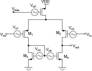
Figure 40 : Opamp input MOSFET noise sources
- Gain from
 and
and  .
.
- Gain from and
 .
.
- Gain from
 and
and  .
.
(This gain factor is relatively small compared to the others, so, it could be ignoredfor further calculations.)
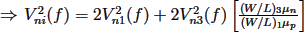
Step 2: Using the gain factors, find the output noise.

Step 3: Find input referred thermal noise voltage by dividing output noise value with gain  which results in
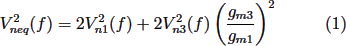
where, 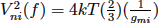

Thus, noise contributed by two pair of transistors is inversely proportional to the transconductance  . Therefore, should be made as large as possible to minimize thermal noise contrinution.
Part (b)
Step 1: In output noise equation, substitute transconductance with transistor size as parameter.
Substituting 
Step 2: Substitute noise sources with spectral density 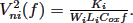
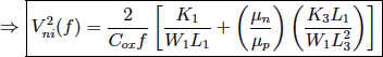
Thus, from the input-referred flicker noise equation,
- Taking
 longer greatly helps due to inverse squared relationship in the second term .
- The input noise is independent of
 and therefore it could be made large to maxi- mize signal swing at the output.
- Taking
 wider also helps to minimize
  noise.
- Taking
 increases the noise because the second term is domnant (due to
  Thus, large decreases the input-referred noise of p-channel drive transistors
which are not the dominant noise source, but, increases the input-referred noise of n-channel
load transistors, which are dominant noise sources.
Thus, large decreases the input-referred noise of p-channel drive transistors
which are not the dominant noise source, but, increases the input-referred noise of n-channel
load transistors, which are dominant noise sources.

